Have a Schematic Ready? What a PCB Layout Designer Needs Before Starting
Before I route the first track, I want to know which decisions the layout is expected to preserve.

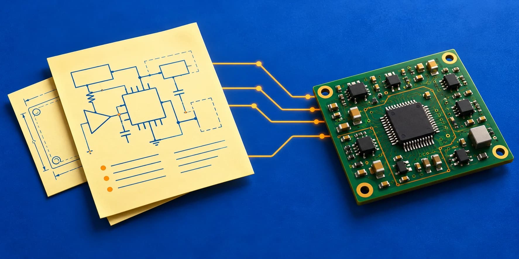
“The schematic is ready. Can you do the PCB layout?” Yes. My next question is what ready means for this particular board.
Are the connector positions fixed? Do the symbols point to the parts you intend to buy? Has someone checked which way the cable plugs in? And when the assembled board arrives, where will we connect a programmer or measure a supply?
Those questions belong at the beginning. A schematic describes electrical connections. A PCB layout turns them into a physical board, where component placement, copper, reference paths, mechanical fit and manufacturing requirements all meet.
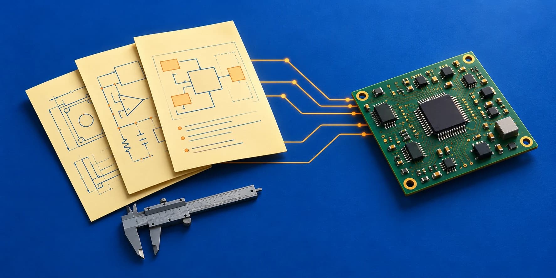
If you already have a schematic and want to hire a PCB layout designer, this is the handoff I would prepare before detailed placement and routing.
What makes a schematic ready for PCB layout
I look for three things: a circuit whose intended operation is understood, component choices that can be checked, and enough physical constraints to begin placement without guessing. The files should agree with each other and identify one revision.
An electrical rule check, or ERC, is part of that preparation. Investigate warnings and record intentional exceptions. A clean ERC report tells us that the configured rules found no remaining violations; it does not establish that every circuit decision is correct or that the product has been tested.
Some decisions can remain open while we discuss the project. They need an owner and a point by which they must be resolved. A connector that may move, an unconfirmed power interface or a pending enclosure drawing can change the layout substantially. I want those dependencies visible before committing to the routing.
Reference: KiCad Schematic Editor reference: electrical rule checking
The files to send your PCB layout designer
Send one clearly named package with the design tool, software version, revision and a short description of what the board does. Include the project-specific dependencies needed to open it. Check that another engineer can identify which files belong together without following a chain of chat attachments.
The table below describes useful inputs. If something is unavailable, say so. Rebuilding a schematic, creating footprints or defining the manufacturing constraints can be included in the work when we agree on it.
| Input | What it helps establish |
|---|---|
| Native Altium or KiCad project, with tool version | Editable connectivity, project settings and the intended source revision. |
| Matching schematic PDF | A readable reference for discussing the circuit and marking review questions. |
| Symbols, footprints and relevant library files | The mapping between schematic pins and the pads that will be manufactured. |
| BOM with exact selected manufacturer part numbers | Which components and package variants the design is intended to use. |
| Dimensioned board outline and mechanical drawing | Mounting holes, fixed connectors, height limits, keep-outs and units. |
| Interface, power and design requirements | Voltage levels, expected loads, constraints and signals needing special treatment. |
| Fabricator or assembler requirements, if selected | Available stack-ups, manufacturing limits and requested release formats. |
| Revision notes and unresolved questions | What is approved, what changed and who will answer the remaining questions. |
What changes if you only have a schematic PDF
A PDF can be enough to discuss the circuit and estimate the next steps. It usually does not provide the editable connectivity, footprint assignments and project settings needed to continue directly into PCB layout.
If the native source is unavailable, the schematic may need to be rebuilt in Altium Designer or KiCad, with connectivity and library choices verified before layout. Existing netlists or other engineering files may help, but their format and completeness need checking.
That is a different starting point from receiving a complete native project. Make the reconstruction work explicit in the scope, and resolve ambiguous labels or missing connections with the circuit owner. A guessed connection should never quietly become an approved requirement.
Check the part and the interface before placement
A component name is not enough to select a footprint. The exact part number, package drawing, pin numbering and intended assembly matter. A symbol and footprint can look sensible separately while mapping a pin to the wrong pad.
Connectors deserve the same attention. Compare the board connector with the mating part, cable and drawing orientation. “Pin 1” should mean the same physical connection in the schematic, footprint, assembly drawing and connected equipment.
Interfaces need more than a net label too. For example, a UART connection does not by itself establish the electrical levels or physical interface. Record the voltage requirements and the device at the other end. Resolve those choices before the layout makes them expensive to change.
In my Altium and KiCad work, I want these checks tied to the selected component documentation. A tidy 3D view is useful for fit; it cannot establish electrical compatibility.
Give the layout a physical boundary and real constraints
A board size alone leaves a lot unsaid. Include mounting-hole locations, connector positions, cable insertion space, component height limits and restrictions on the underside. A STEP model can help, alongside an agreed dimensioned drawing. Mark which positions are fixed and which are suggestions.
An illustrative example: a connector can fit inside the board outline while its cable cannot be inserted once the board is in the enclosure. That becomes a placement constraint before routing, rather than an assembly surprise afterward.
Next, identify constraints that affect placement, stack-up and copper: power demand, switching circuits, sensitive measurements, wireless areas, isolation requirements and interfaces needing controlled impedance or other routing rules. Apply the requirements for the actual circuit instead of giving every signal the same treatment.
Layer count belongs in this discussion. If it is fixed, state that constraint and why. If it is open, review the circuit, outline and manufacturer's available stack-up before choosing. When controlled impedance is required, define it against the intended construction rather than copying a track width from a different board.
I also want programming, reset and useful measurement access considered while there is still room to place it. If the board does not boot, where will the engineer start checking? That question can change a placement decision today.
Agree on what the layout engineer can change
A layout-only engagement should still have a way to raise circuit questions. It should be clear whether schematic review is included, who approves a component substitution or pin change, and how those changes return to the source files.
I prefer a short issue list with the location, concern, required decision and owner. Some findings need resolving before placement. Others need a decision before routing or final release. Agreeing on those checkpoints keeps a review from becoming a collection of unanswered comments.
Also separate hardware design from firmware, enclosure work, purchasing, fabrication, assembly and prototype testing. Include the responsibilities you actually need in the quotation. A PCB file review does not demonstrate that an assembled product works.
Plan the review and manufacturing handoff
For a new layout from an existing schematic, agree on review points before work starts. A useful sequence is to confirm the inputs and open questions, review placement against the mechanical constraints, review the routed board, and check the exported release package.
Run the relevant design checks, investigate errors and document approved exceptions. Then inspect the outputs that will actually go to the manufacturer. The schematic, board, BOM and assembly information should describe the same released revision.
The deliverables depend on the agreed work and the selected manufacturer's requirements. Confirm them rather than assuming that “PCB files” means the same thing to everyone.
- Editable schematic and PCB project, with the required project-specific libraries.
- Schematic PDF and the agreed bill of materials.
- Fabrication data, such as Gerber and drill files, with the required stack-up and fabrication notes.
- Assembly data, such as pick-and-place files and assembly drawings, when assembly is in the handoff scope.
- Agreed mechanical exports, check summaries and a record of unresolved or accepted items.
- A release identifier that connects the source revision to the files being shared.
Reference: KiCad PCB Editor reference: design checks and manufacturing outputs
A handoff checklist you can use before sending the files
You do not need to polish every document before making contact. Start with the latest files and a clear account of what is confirmed. Mark missing inputs as “to be confirmed” and identify who will supply them.
I would rather know that the enclosure drawing is still changing than route around an outline everyone assumes is final. A useful handoff makes that distinction easy to see.
- One sentence describing the product and what the board must do.
- Requested work: layout only, schematic review plus layout, or reconstruction plus layout.
- Design tool, version and source revision, with the matching PDF, BOM and libraries.
- Board outline, mounting, connector and height constraints, labelled fixed or provisional.
- Power, interface and routing requirements, with unresolved decisions listed separately.
- Manufacturer requirements and layer-stack information, where available.
- Expected deliverables, review contacts, change-approval owner and target dates.
Common questions before starting PCB layout
| Question | Practical answer |
|---|---|
| Can PCB layout start from an existing schematic? | Yes. First check the source files, libraries, component assignments and physical constraints, and agree on any review or correction work needed. |
| Is a schematic PDF enough? | It can support the initial discussion. If editable engineering data is missing, rebuilding and verification may be required before layout. |
| Can a schematic from one EDA tool be laid out in another? | Potentially, but assess the transfer first. Connectivity, libraries, footprints and constraints need verification, and migration may add work. |
| Does a clean ERC or DRC report prove the board will work? | No. Those checks evaluate configured rules. Circuit review, mechanical verification and physical testing address additional questions. |
| Can you quote a layout without every detail being final? | An initial discussion can identify the likely scope. A firm fee and delivery commitment need enough confirmed inputs and clear treatment of open decisions. |
Working with me on an existing schematic
I am Dhara Rajpura, a PCB design and embedded hardware engineer working with Altium Designer and KiCad. I can help turn an existing schematic into a PCB layout and an agreed manufacturing package, or discuss a review first when the circuit still has unresolved questions.
Send the source files you have, the board's physical constraints and the part of the project you are least certain about. We can identify what is ready, what needs a decision and what the layout engagement should include before routing begins.
Technical references
Use the documentation for your installed EDA version and the datasheets for your selected components alongside this checklist.

Dhara Rajpura
Freelance PCB design and embedded hardware engineer working with Altium Designer and KiCad. Explore my documented project scope and engineering services.
About Dhara ↗