Services / 01—04

Focused hardware services, built around a clean handoff.

Choose a defined engagement or bring a product challenge. Every scope starts with constraints, ends with usable engineering files, and stays honest about its boundaries.

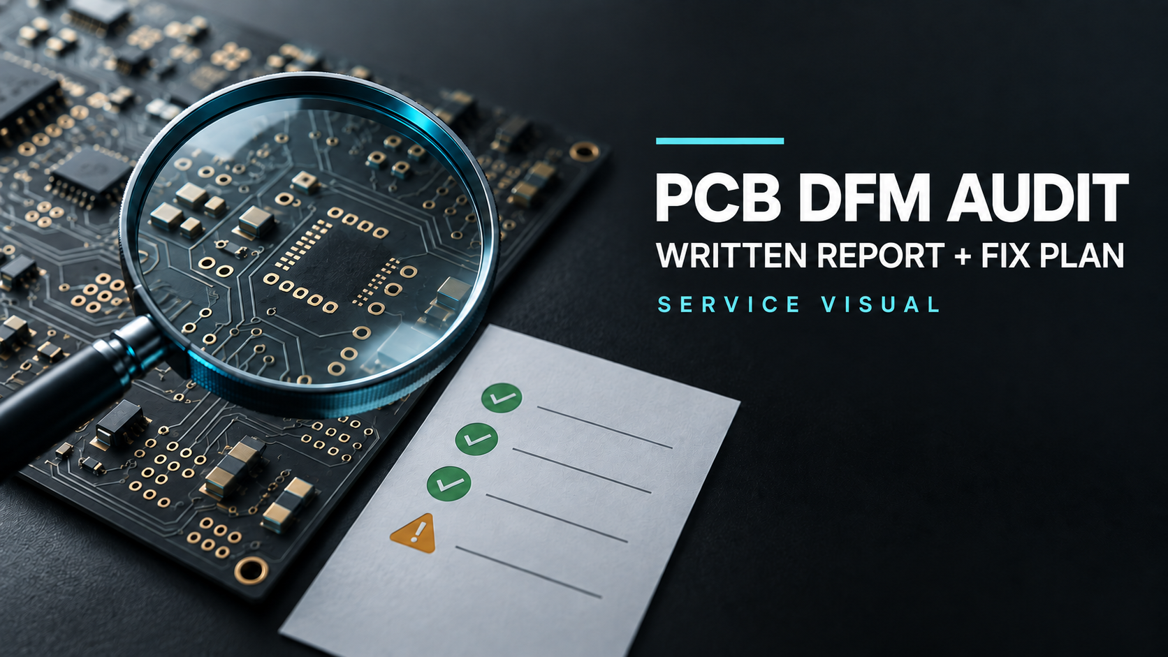
PCB Design Review & DFM Audit service visual
01
Engineering service

PCB Design Review & DFM Audit

An independent review of schematic, layout and fabrication readiness before files reach the factory.

What I handle

  • Schematic and layout review
  • Power, grounding and return-path analysis
  • DFM / DFA checks
  • Prioritized findings with clear actions

Deliverables

  • Annotated review report
  • Risk-ranked issue list
  • Manufacturing-readiness notes
Scope boundary

Review and recommendations only; redesign, firmware and certification management are separate scopes.
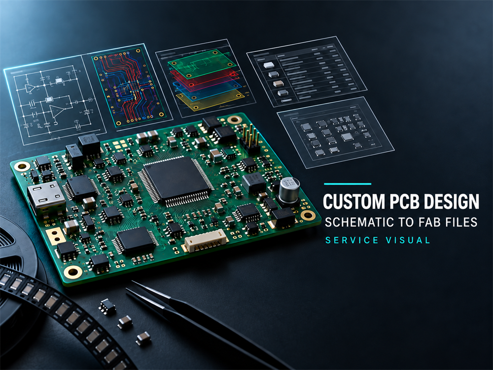
Production-Ready Custom PCB Design service visual
02
Engineering service

Production-Ready Custom PCB Design

A complete board implementation structured around product, mechanical and manufacturing constraints.

What I handle

  • Requirements and system partitioning
  • Schematic capture and design checks
  • Placement and multilayer routing
  • Release-package preparation

Deliverables

  • Native design files
  • Gerbers / ODB++, drill and drawings
  • BOM and pick-and-place data
Scope boundary

Firmware, enclosure design, procurement, assembly and certification management are not included unless separately agreed.

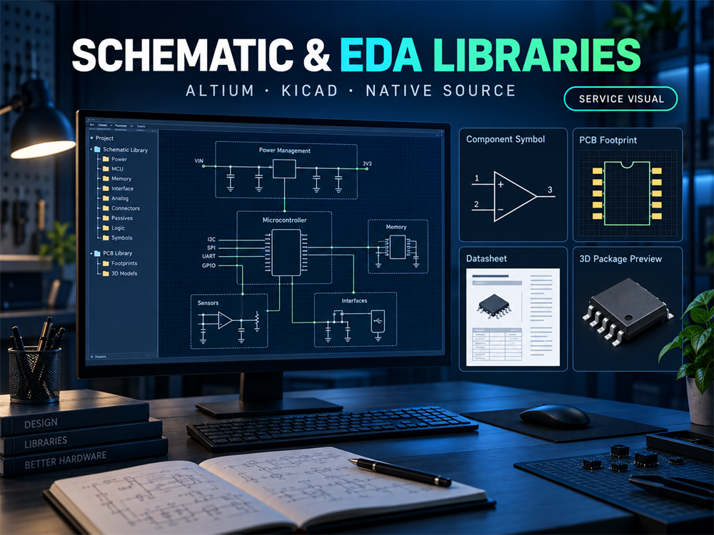
Schematic Capture & EDA Library Creation service visual
03
Engineering service

Schematic Capture & EDA Library Creation

Clean, editable engineering data from PDFs, legacy designs, datasheets or early circuit notes.

What I handle

  • PDF and legacy schematic rebuilds
  • Hierarchical schematic organization
  • Custom symbols and footprints
  • ERC and library verification

Deliverables

  • Native EDA project
  • Annotated schematic PDF
  • Verified library, BOM and netlist
Scope boundary

PCB layout and functional validation are outside this service unless added to the project scope.

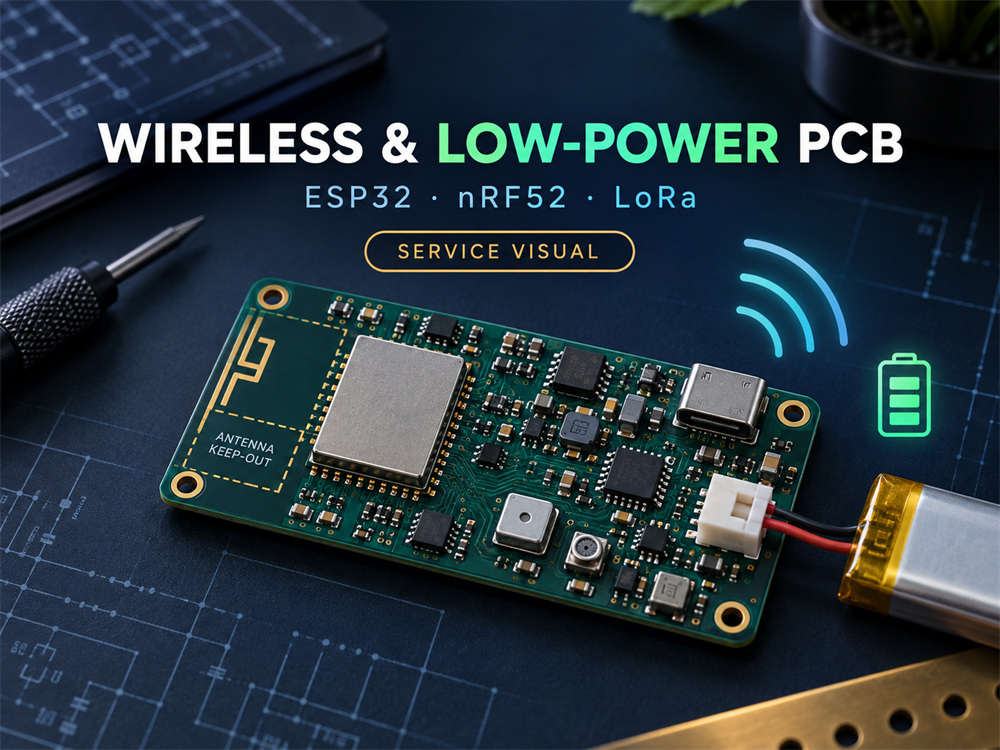
Battery-Powered Wireless / IoT PCB service visual
04
Engineering service

Battery-Powered Wireless / IoT PCB

Low-power connected hardware for ESP32, nRF52, LoRa, USB-C and LiPo-based products.

What I handle

  • Radio and power architecture
  • Charging and current-budget planning
  • RF-aware placement and routing
  • Antenna keep-outs and grounding strategy

Deliverables

  • Schematic and PCB files
  • Manufacturing package
  • Power notes and DFM checklist
Scope boundary

Laboratory RF tuning, firmware, compliance testing and guaranteed range or battery life are not included.

Process / 04 stages

A disciplined path to release.

  1. 01

    Define

    Interfaces, mechanics, power, parts and manufacturer limits.

  2. 02

    Capture

    Architecture, schematic and component-library verification.

  3. 03

    Implement

    Placement, routing, planes, checks and focused reviews.

  4. 04

    Release

    Native files and a complete manufacturing package.

Start with context

Tell me what exists—and what must ship.

Share a block diagram, schematic, mechanical constraints or current board files. I’ll help define the right hardware scope.

Discuss your project ↗