PCB Design Review Before Manufacturing: A Practical Checklist
A clean DRC report is a useful checkpoint. A release decision needs a wider view of the circuit, the assembly and the files you are about to send.


The routing is finished. The board looks tidy in 3D. You are one export away from sending it to the manufacturer. This is a good moment to pause and ask a different question: what evidence says this particular revision is ready to build?
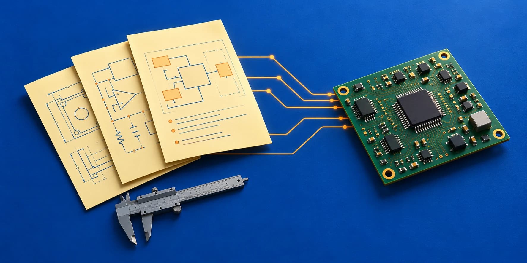
A PCB design review connects the circuit requirements to the physical board and the manufacturing package. It looks for issues a design-rule check may not capture, such as a wrong connector orientation, an unsuitable footprint or an undocumented assembly option.
Use this checklist for a structured review before fabrication. Adapt it to the circuit, component datasheets, manufacturer capabilities and project requirements. A file review improves release readiness; prototype bring-up and any required compliance testing still need their own plan.
1. Freeze the revision you are reviewing
Start with a matched set of schematic, PCB, libraries and BOM. Include the intended board stack-up, mechanical drawing and manufacturer rules. Record the revision and review scope before editing starts.
A review of a PCB screenshot is limited because it cannot reliably establish connectivity, hidden layers or the configured constraints. Native Altium or KiCad files allow a more complete inspection. If only PDFs or manufacturing files are available, state those limits in the report.
Keep a short issue log: location, concern, likely impact, proposed action and owner. For example, an unconfirmed mating connector is a release question, not a note to quietly resolve after ordering boards.
2. Check the schematic—and the part that will actually be assembled
Follow the main functions from supply input to the loads and from each external connection to the controller. Check voltage compatibility, pin assignments, reset and boot requirements, protection and programming access against the selected parts’ datasheets.
Pay particular attention to connectors, polarized parts and custom libraries. Verify the manufacturer part number, package drawing, pin numbering and footprint orientation. Similar-looking packages or top-view and bottom-view drawings can lead to mistakes that a neat 3D render will not reveal.
Run electrical rule checking and investigate its warnings. A deliberately unused pin and an accidentally unconnected pin should not be treated as the same decision. Document intentional exceptions rather than suppressing a category of warning simply to obtain a clean report.
- Selected part numbers, schematic symbols and footprints agree.
- Connector pinouts are checked against the mating device and cable.
- Polarity and pin 1 are clear in the design and assembly information.
- Programming, reset, boot and essential test access are available.
- Assembly variants and do-not-populate parts are documented.
Reference: KiCad reference: electrical rule checking
3. Review power paths and signal return paths together
For each rail, review the source, load demand, protection, copper path and expected operating conditions. Consider startup and peak loads as well as nominal operation. Check capacitor voltage ratings, regulator thermal requirements and the component manufacturer’s layout recommendations.
In a buck converter, inspect the placement of the input capacitor and the high-current switching loop. Keep sensitive feedback routing away from the switching node and follow the regulator-specific guidance. Texas Instruments’ step-down converter layout guide explains why these placement and routing decisions matter.
For signals, inspect the nearby reference copper and the route their return currents can take. Plane gaps, layer changes and connector transitions deserve attention. Separating analog and switching areas requires a considered return-path strategy; dividing ground copper without analysing current flow can introduce new problems.
Mixed-signal systems such as a load-cell measurement board or a motor-control board need this wider review. The schematic connection alone does not describe how switching currents and a sensitive signal path share the physical layout.
Reference: Texas Instruments: five steps to a great step-down converter layout
4. Check what the enclosure, cables and antennas change
Compare the PCB outline and holes with the agreed mechanical drawing. Inspect component heights, screw-head clearance, connector insertion space and access to buttons, batteries and test points. A component that fits on the board can still be inaccessible inside the enclosure.
For wireless designs, check the selected module or antenna’s placement and keep-out requirements. Review nearby copper and metal, the enclosure arrangement and any RF connector or feed details. Follow the actual hardware vendor’s guidance instead of applying a universal antenna clearance.
Where controlled impedance is needed, use the intended fabrication stack-up and agreed constraints. Track width cannot be chosen reliably from a screenshot or layer count alone. Confirm any impedance requirements with the board manufacturer before release.
5. Run DRC with rules that match the intended build
Set fabrication constraints from the selected manufacturer’s capabilities and the project’s requirements. Check clearance, track and drill dimensions, board-edge spacing and relevant net-specific rules.
In KiCad, refill copper zones and run DRC with schematic-to-PCB parity checking where applicable. Review rule violations, unconnected items and exclusions. Save the report with the release record.
DRC checks the constraints and connectivity represented in the design. It cannot establish that every engineering requirement has been correctly entered. Follow it with an assembly review: part access, placement orientation, markings, solder-mask and paste details, and any special process requirements.
Reference: KiCad reference: design rule checking and fabrication outputs
6. Review the exported package, not only the editor
Generate the manufacturing outputs from the approved revision, then open them in an appropriate CAM or Gerber viewer. Check the board outline, copper layers, solder mask, silkscreen and drill alignment. Include plated and non-plated hole information in the format your manufacturer requires.
For assembly, cross-check the BOM and placement data against the board. References, manufacturer part numbers, fitted quantities and assembly variants must agree. Confirm the assembler’s expected origin, units and rotation conventions; a file that exports successfully is not automatically interpreted correctly.
Place the files in one clearly named release folder with the revision, date and any fabrication or assembly notes. Remove obsolete outputs from the package. If a review causes a change, regenerate all affected files and recheck the package before sending it.
A practical release checklist
Make the review actionable. Use the table below as a release record, adding evidence and an owner to each line. An unresolved power, pinout, mechanical or manufacturing question should have an explicit release decision.
- Every blocking issue is resolved or the release is held.
- Accepted exceptions have a reason and an accountable approver.
- All deliverables refer to the same approved revision.
- The team knows who will order, assemble and test the prototype.
| Checkpoint | Evidence to retain |
|---|---|
| Revision and requirements | Matched project files, requirements list and agreed review scope |
| Circuit and libraries | Reviewed datasheets, pinouts, footprints and ERC findings |
| Power and layout | Review notes for load paths, thermal concerns, returns and critical signals |
| Mechanical and manufacturing | Outline/assembly checks and manufacturer-specific constraints |
| Rule checking | DRC results and explained exceptions |
| Release package | Viewed exports, consistent BOM/placement data and revision identifier |
| Approval and next steps | Issue owners, release approval and prototype bring-up plan |
When an independent review helps
Another engineer can be useful before a first fabrication run, after a major revision or when a design is being handed to a new manufacturer. Agree whether the review covers the schematic, layout, manufacturing outputs or all three.
Ask for a prioritized report rather than a general verdict. A useful finding points to the relevant component or region, explains the concern and identifies the action needed. Review and redesign should be agreed as separate responsibilities so it is clear who will make and verify changes.
For my PCB design review service, send your current files, product requirements and the questions you want examined. We can define the review boundary and deliver a focused set of engineering actions before the board goes to fabrication.
Technical references
Use the documentation for your installed EDA version and the datasheets for your selected components alongside this checklist.

Dhara Rajpura
Freelance PCB design and embedded hardware engineer working with Altium Designer and KiCad. Explore my documented project scope and engineering services.
About Dhara ↗